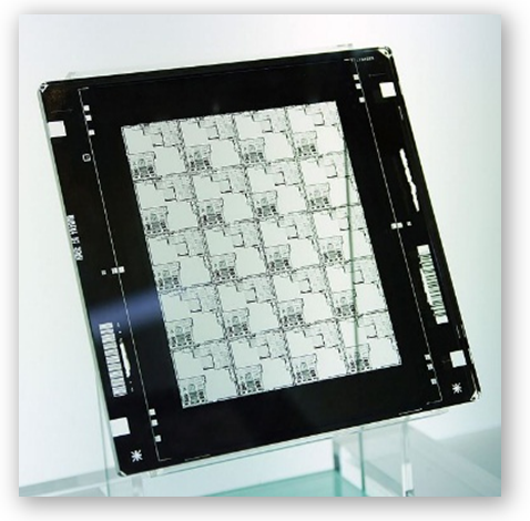
Photomask defect classification is time consuming, costly, and prone to occasional human errors causing millions of dollars in lost wafers every year.
ADAS accurately automates defect classification and measurement, increasing throughout and dramatically reducing the risk of missed yield-limiting defects printing on wafers. ADAS is compatible with all mask inspection tool manufacturers including Lasertec, KLA-Tencor, Applied Materials, and NuFlare.
-ADAS is the only commercial automatic defect classification system in wafer fab production with no known misclassified critical defects
Pass/Fail criteria is determined in part by:
A question constantly asked in wafer fabs is, "Will this defect print?" Such uncertainty causes production masks to be put on hold for hours or days while expensive print checks are performed.
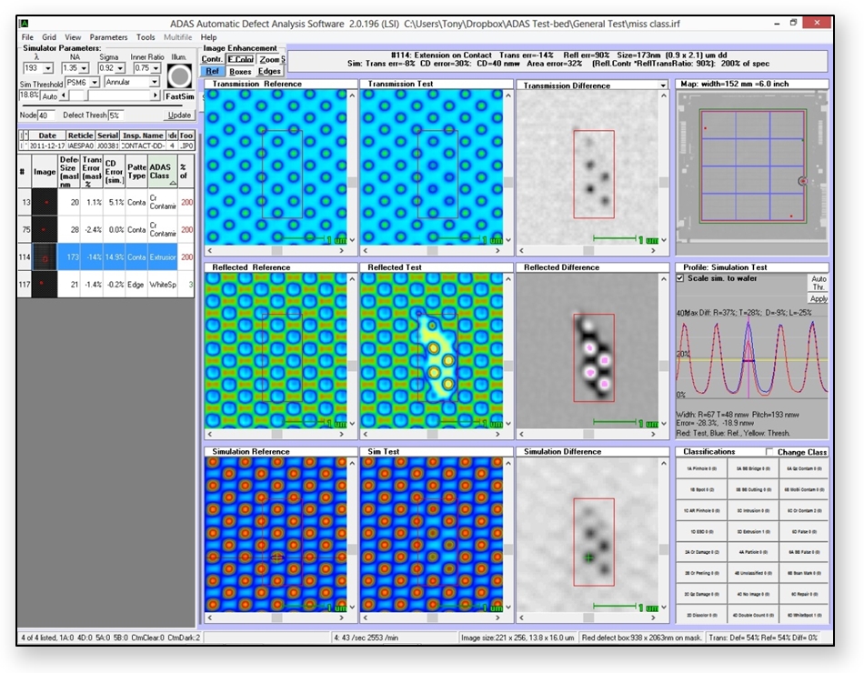
—In order to assist in predicting defect printability, ADAS incorporates an aerial image simulator which greatly reduces the risk of yield limiting defects entering wafer production
ADAS' patented printability simulator provides:
Critical mask inspection are run at high sensitivity to ensure detection of all defects. These aggressive settings can produce very high defect counts, greatly increasing the risk of misclassification and long mask hold times.
—ADAS analyzes over 1,000 defects per minute allowing inspection tools to be run at high sensitivity ensuring detection of all critical defects without decreasing inspection area efficiency

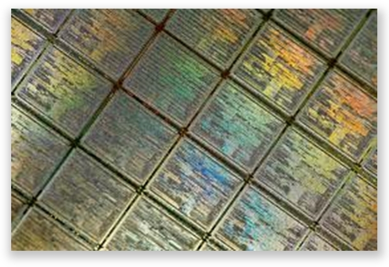
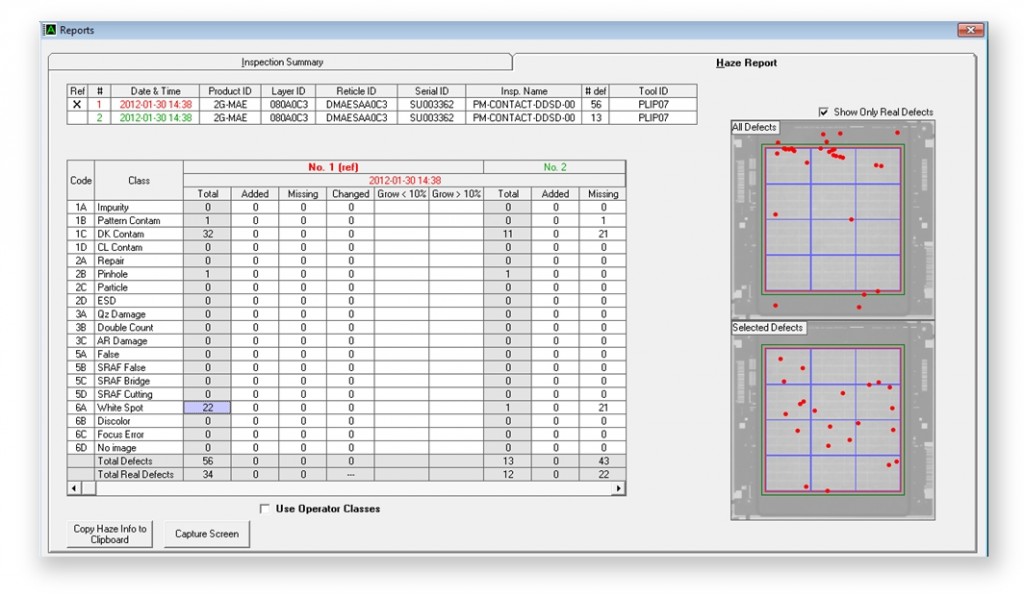
High exposure in ArF scanners frequently leads to haze defects which can rapidly kill wafer yields.
—ADAS automatically provides early detection of these growths by comparing defect locations and sizes to past inspections, easily identifying changes to the photomask
Analysis tools provide:
Does it work with my inspection tools?
— Yes. ADAS is compatible with Lasertec Matrics (x600, x700, x800), K-T (3xx, SLF, 5xx, 6xx), NuFlare.
How fast is it?
— Very Fast! ADAS processes over 1,000 defects/minute.
How accurate is it?
— ADAS is so reliable that most inspections do not require operator review. No known missed critical defects.
How does the simulation work?
— AVI uses a patented single pass method customized for optical mask inspection tools.
Is it easy enough for operators to learn and use?
— The user interface is customized for each fab and user: Concise screens for operators and detailed screens for engineers.
What is the output? Can I export data to Excel?
— The system can export data in KLARF, LRF, or Excel compatible file formats.
Is it compatible with my YMS system and/or SECS/GEM?
— Custom YMS interfaces are written for each customer.
How flexible is it with new designs or shrinks?
— Normally, no changes are required to handle new designs and shrinks.