Improved
Method for Measuring and Assessing Reticle Pinhole Defects for the 100nm
Lithography Node
Darren Taylor
Photronics, Allen TX 75013
Anthony Vacca, Larry Zurbrick
KLA-Tencor, 160 Rio Robles, San Jose, CA 95161
ABSTRACT
With the approach of the
100nm-lithography node, an accurate and reliable method of measuring reticle
pinhole defects becomes necessary to assess the capabilities of high-end
reticle inspection equipment. The current measurement method of programmed
defect pinholes consists of using a SEM.
While this method is repeatable, it does not reliably represent the true
nature of a pinhole.
Earlier studies have suggested that since the SEM images only a top down view of the pinhole, the measurement does not accurately account for edge wall angle and partial filling which both reduce pinhole transmission and subsequent printability. Since wafer lithography and reticle inspection tools use transmitted illumination, pinhole detection performance based on SEM measurements is often erroneous.
In this study, a pinhole test
reticle was manufactured to further characterize the capabilities of a
transmission method to measure pinholes.
Keywords: Inspection, Pinhole, Printability
1.
PROBLEM DEFINITION
Because of the inability to reliably manufacture and
measure programmed pinhole
defects on test masks,
some reticle inspection tool vendors have stoppedshied away from
setting a specification on these types of defects. This has left a hole in
setting specifications from the customer of the mask houses.
From 1979 to the present, optical shearing microscopes were used to
measure these defects. The resulting measurements were used in multiple
printability studies in the industry. This method was adequate when the size of
the defects were relatively large, however, issues began to arise when the when
the defects fell below 500nm. The repeatability of the measurements became poor
below 500nm and very poor below 200nm. In 2000 KLA-Tencor migrated to using a
KLA-Tencor 8100XPR CD-SEM to measure the defects. This was done primarily for a
high repeatability. The sizing method is the inscribed circle method. This
involves placing a circle inside the defect and reporting the size of the
defect. This methodology was chosen due to thebecause it has pretty
good correlation back to the historical optical sizing1..
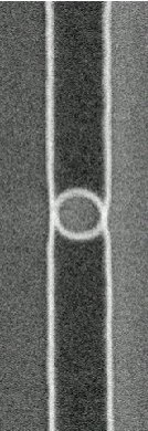
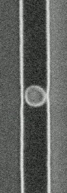
While SEM measurement are highly repeatable there
are issues with this type of measurement. It cannot take into account poor
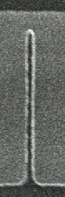
sidewall or the presence of debris in the bottom of the pinhole. An example of
this is shown in Iimage
1.
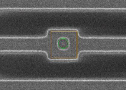
Image 1.
CD-SEM Circle
Inscribed Methodology
The green circle is where the measurement was taken.
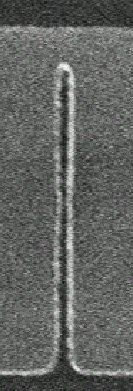
As shown in the image there are very poor sidewalls on the defect. Image 2
shows an example of a "good" defect. This defect has a relatively
high sidewall angle and is completely cleared.
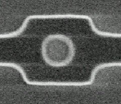
Image 2.
Example of a
"good" pinhole
As the test mask geometry and defect sizes shrink s, and
therefore the defects present, have become increasingly aggressive it
has become necessary to find a new measurement protocol to overcome the issues
seen with the SEM measurements. Several methods were investigated such as probe
type metrology, SEM improvements and transmission based metrology. There are
issues associated with each of these. Probe type metrology is interesting but
the size of the tip approaches or is larger than the defect of interest. SEM
metrology could be improved to capture a better point in the sidewall, however,
it does not address the issue of foreign material in the defect. Transmission
based metrology appears to be the most comprehensive of the three and it moreis closely resembles r to
the actual function of the mask in optical lithography.
Two transmission based measurement tools were
investigated in this, an ongoingthis ongoing study of
the issue, the KLA-Tencor Defect Energy Meter and the AVIÔ Flux-Area Measurement tool. The KLA-Tencor DEM is an engineering mode
tool that uses images from an SLF27 inspection tool to measure the defects. A special noncommercial extraction program was written
that enabled the The AVI tool to uses the same images. but obtains them from a
results file. Both measurement techniques were shown to be
repeatable within a single tool and from tool to tool in an earlier study on
this problem2..
The decision was made to use the AVI tool primarily
because it has the ability to create a reference within the defect image and
the KLA-Tencor DEM tool needs a separate reference image. KLA-Tencor has the
ability to capture images of the defects manually on the SLF27, however, only the
defect image is captured, the reference image is not fully aligned which is
necessary for the needed by the DEM to functionis not
stored.
2.
EXPERIMENT
A programmed defect test mask based on the
KLA-Tencor UTM was built using a 50KeV-lithography tool. The plate was designed
for the 100nm node. The main feature size was 400nm and the defects were in
increments of 20nm. The basis for the test plate was the KLA-Tencor UTM, this
is the mask design that
KLA-Tencor intends to use for setting the detection rate specifications on the 5XX generation tool.
This test mask was inspectedran multiple
times on several KLA-Tencor SLF27 inspection tools and measurements made usingon the AVI tool
on the individual runs. Chart 1 shows the repeatability of the AVI pinhole measurements from system to
system. The X axis shows the average defect size measured with the AVI software
while the X axis shows the variation from the average for each individual
system. The data show less than ±3nm variation all the way down to
the 116nm sized pinhole.
Sensitivity measurements were taken from the
inspection tools and the results are shown in image 5. The gray area in the
sensitivity chart represents 100% capture rate. The individual boxes show the
actual capture rate for that particular defect.
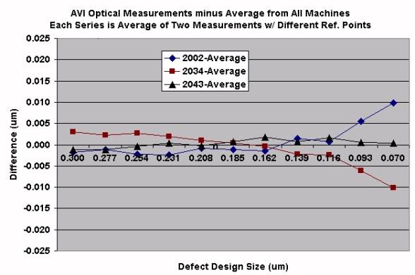
Chart 1Image 3.
AVI System to System Measurement
Repeatability
Chart 2 shows the relationship
between the AVI measured sizes and the CD-SEM sizes along with the delta
between them. The delta has a range of 13nm. The yellow bar in the chart shows
the 100% capture point for the SLF27 tool.
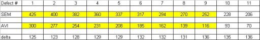
Chart 2Image 4.
SEM vs AVI measurements
Image 4 shows the relationship between the AVI
measured sizes and the CD-SEM sizes along with the delta between them. The
delta has a range of 13nm. The yellow bar in the chart shows the 100% capture
point for the SLF27 tool.
Sensitivity measurements were taken from numerous
inspection tools and the results from one system are shown in Chart 3. The gray area in the
sensitivity chart represents 100% capture rate. The individual boxes show the
actual capture rate for that particular defect. The average defect sizes as measured by
the AVI are shown along
the right side vertical axis
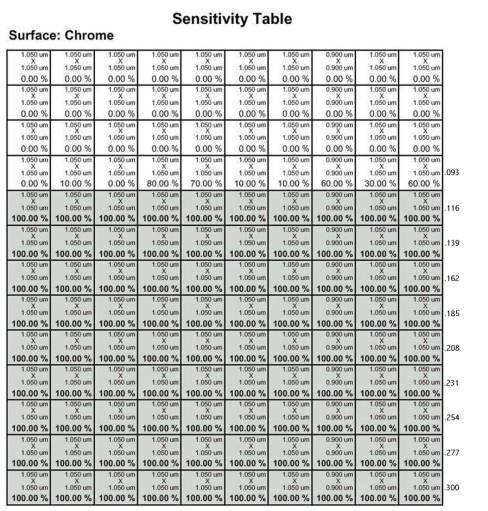
Chart 3Image 5.
SLF Pinhole
Sensitivity from Test Mask
3.
PRINTABILITY
In earlier phases of this study printability was
performed to get a sense of how transmission measurements compared to
printability. A test mask designed for the 130nm node (520nm lines) was printed
with aggressive low k1 lithography
(~ .42).
Defect 12 Defect
12-wafer Defect 11 Defect 11-wafer
Images 36 through 69.
Printed Images
for 130nm node
Images 36 through 69 show two consecutive defects on a
programmed defect mask. There are two pair of images, one SEM image of the mask
and the other is the SEM image of the printed wafer. The SEM circle inscribed
method measurement on defect 12 was 215nm and the SEM measurement for defect 11
was 212nm. The AVI measurements for the same defects were 183nm and 114nm
respectively. As shown in on the wafer images, defect 12 on the mask printed on
the wafer causing the line to pinch. Defect 11 on the other hand did not print
although the SEM measured only 3nm difference between them. The AVI measurement
showed a difference of 69nm, which would be in better agreement with the
printing results.
In the case of isolated pinholes the largest pinhole
on the mask, which measured 279nm by SEM and 155nm by energy measurement, did
not print.
The printability results suggest that the capture
rate of the KLA-Tencor SLF27 tool is well below the printing threshold. The SLF
captured the defects in the 116nm range 100% of the time. It also shows that the
repeatability of the AVI tool is stable well below printing levels.
4.
SUMMARY
Large strides have been made in overcoming the obstaclesability in to repeatablebly measurement of small programmed
pinhole reticle
defects. The AVI transmission
based measurement method, AVI, that was chosen in
this study showed good repeatability on very small defects far below what actually
prints. The KLA-Tencor SLF27 system also demonstrated the ability toshowed a
capture
rate on pinholes far below the printing threshold.
5.
REFERENCES
1 L.
Zurbrick, et al, “Reticle defect size calibration using low-voltage SEM and
pattern recognition techniques for sub-200 nm defects”, Proc. SPIE Vol. 3873,
p.651-658, 19th Annual Symposium on Photomask Technology, F. E.
Abboud; B. J. Grenon; Eds. (1999)
2 D. Taylor, et al, "Improved
Method for Measuring and Assessing Reticle Pinhole Defects", Proc. SPIE
Vol. 4562, p. 272-278, 21st Annual BACUS Symposium on Photomask
Technology, G. T. Dao; B. J. Grenon, Eds. (2002)
L. Zurbrick, et al, “Reticle defect size
calibration using low-voltage SEM and pattern recognition techniques for
sub-200 nm defects”, Proc. SPIE Vol. 3873, p.651-658, 19th Annual
Symposium on Photomask Technology, F. E. Abboud; B. J. Grenon; Eds. (1999)
6.
ACKNOWLEDGEMENTS
Matthew Lassiter, Ben Eynon - Photronics
Mohsen Ahmadian, Ed Longboy, Lantian Wang -
KLA-Tencor
Peter Fiekowsky - AVI
IMEC for graciously printing wafers for this
project